Dear manager,
Nice day!
This is Anne from Shenzhen JSD PCB Technology CO., Ltd.. It has been established for 20 years. We are the leading
prototype, Small Volume, Superior Difficulty, High Precision, High Quality PCB Manufacturer.
Our strengths as follow:
1.Quick response, JSD PCB will reply Customer's enquiry within 1 hour;
2.More than 200 type of PCB can be worked out Every day;
3.Board thickness VS drill size: 16:1
4.Line width/spacing: 2/2mil
5.Min hole size: 0.1mm(laser drilling)
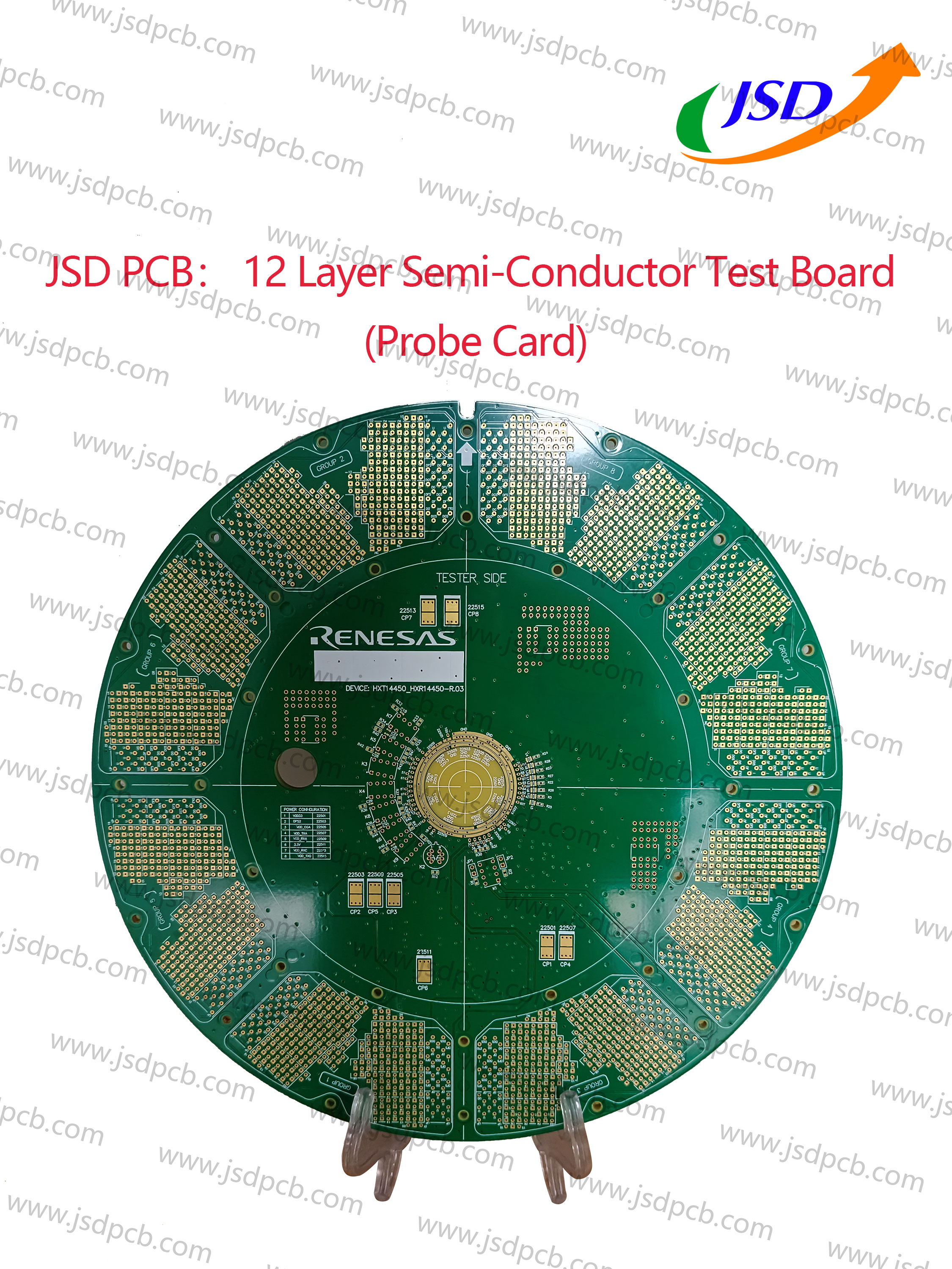
Share a PCB picture with you——12 Layer Semi-Conductor Test Board (Probe Card)
If you have any requiries or questions, please feel free to contact with us.
Best regards,
Anne
Shenzhen JSD PCB Technology Co., Ltd.
Email: Anne@jsdpcb.com
Website: www.jsdpcb.com
Ph/Skype/Wechat: +86-17092791810
Factory Base: Building 12,LiSheng Industrial Area,
TangWei,Bao'anDistrict,Shenzhen,GuangdongProvince,P.R.China
P Think Green! Before printing this e-mail.
|
|

|